

What is (Laser-)Depaneling?
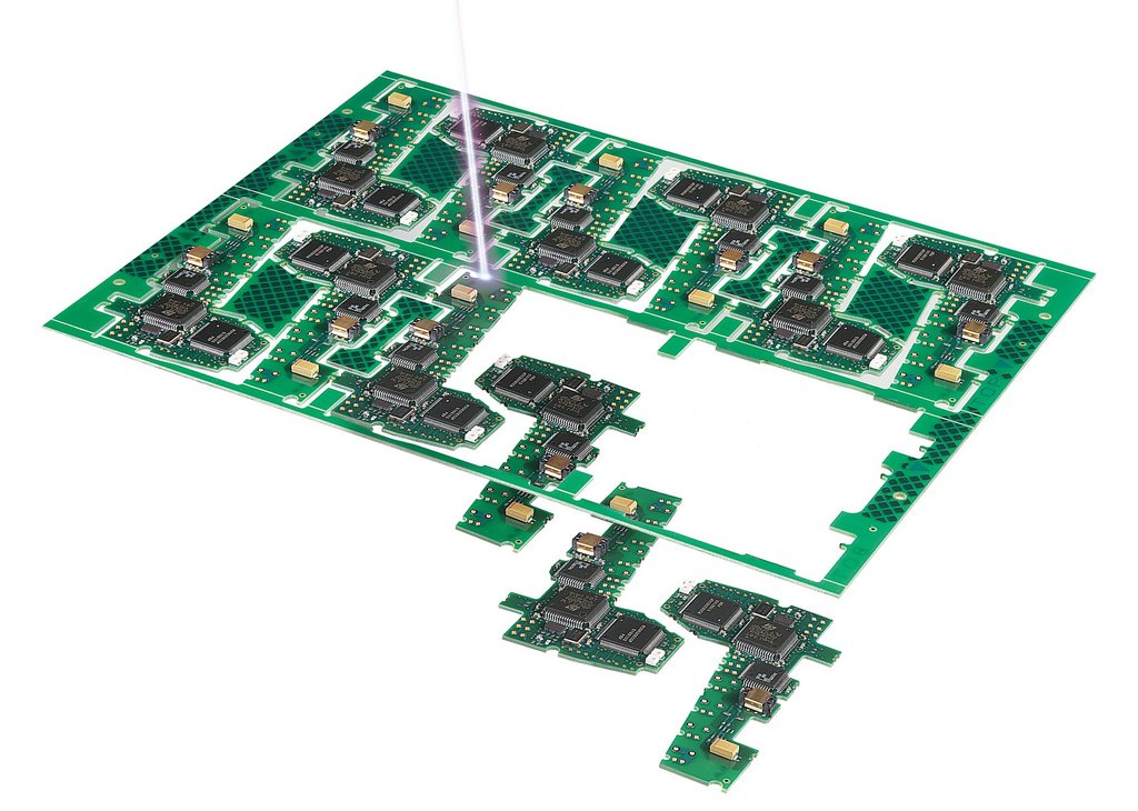
Laser Depaneling is one of the most modern and promising processes for separation PCBs from the overall panel. During the depaneling process, the previously manufactured and assembled printed circuit boards (PCBs) are cut out of the panel using a suitable separation process/tool. In the case of laser depaneling, the singulation process is performed by a focused laser beam that ablates the material layer by layer. The laser method - especially applied by LPKF machines - offers significant advantages compared to conventional mechanical separation methods.
Laser cutting PCBs: How does the process work?
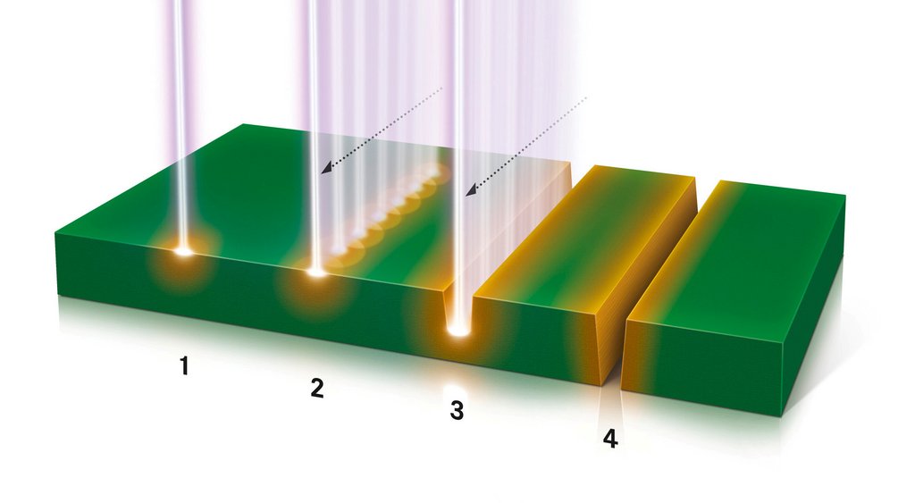
In case of laser depaneling, the thermal energy of the laser is used to remove the material path by path / layer by layer. With each repitition, a pre-defined thickness of the material is ablated and vaporised. The resulting fumes are extracted during the process by a powerful suction system. Due to the small particles and the powerful suction, the deposition of residues is reduced to a minimum. In addition, the thermal energy is regulated during the entire process in such a way that, depending on the specific requirements, there is no or only very little carbonisation of the material.
Due to the layer-by-layer ablation process of the laser, it is not only possible to cut through the boards completely, but also to remove individual layers or predefined thicknesses of the material. Due to the precision and filigree of the laser, ablations can be performed with an accuracy of a few µm.
Choose from the LPKF System Portfolio
Various laser options and different system characteristics allow you to find the right balance between cost and quality for your depaneling applications, depending on the field of usage. LPKF laser technology is highly productive for both special applications and large series. We will gladly assist you in selecting the perfect solution for you with regard to our range of options:
- Laser sources: ultraviolet and green lasers with pulse durations in nano- and picosecond range
- Working area: small and large working areas covering all standard formats
- Automation level: stand alone or as part of a fully automated and/or integrated production line


Application Diversity of Laser Cutting
Different applications of Laser Cutting
Different material combinations of FR4 composites can be processed with the laser without any problems. It is possible to achieve combinations of cutting edge quality and effective cutting speed that cannot be achieved with any mechanical cutting processes. In addition, the laser technology does not cause any mechanical stress in the material due to the non-contact functional principle, and there is no dust deposition on the surface due to the process, which could result in malfunctions.
In comparison to traditional separation methods, the laser process can be used to cut a wide variety of material thicknesses and compositions of flexible PCBs with maximum cleanliness, care and precision. In the process, the tool leaves no traces on neither the laser entry side nor the laser exit side that might have a bad influence on the quality of the substrate or the entire circuit board.
The main advantage of the laser process over the traditional mechanical cutting methods is the wear-free processing. It is due to the fact that extremely high hardness of the materials is not relevant for the laser ablation process. In addition, the use of lasers enables the clean cutting of complex structures of ceramic circuit boards and molded parts in various material thicknesses. The parameter settings of the laser allow the individual requirements of the ceramic circuit boards to be taken into account easily.
The solution developed by LPKF to meet the special requirements of IMS machining offers a lot of advantages. The benefits for the customer include the fact that the material is not mechanically stressed, no metal chips can be deposited and the cutting edge quality and effective cutting speed are correspondingly high.
Answers to possible questions:
FAQ about laser depaneling
There is a widespread prejudice that laser systems are expensive and not sufficiently cost-efficient. However, this assumption is now outdated, because the price-performance ratio of the systems has improved by a factor of 10 over the last decade. Consequently, laser systems are highly attractive for a very wide range of applications. Compared with milling machines, they are nowadays at a comparable price level in terms of investment costs and score particularly well for their low follow-up costs. There are no regular costs for wear parts such as milling heads or saw blades, there are inexpensive universal workpiece carrier solutions, and the material used can also be used much more effectively.
Another common prejudice is that the laser would burn or inevitably carbonize the PCB material. Here, too, the world now looks quite different: LPKF's CleanCut and Tensor technology in particular help to specifically control the heat input into the material. In this way, carbonization can be allowed or completely excluded, depending on the requirements. Even components very close to the cutting channel are not damaged by the energy introduced by the laser. External investigations for our systems prove that even 100 µm away from the cutting channel temperatures are measured that are far from damaging components.
A frequently asked question is also the speed of depaneling with the laser. This question can hardly be answered in a general way, but requires a more differentiated consideration. The speed depends on several factors: the laser variant, the type and thickness of the substrate, and the desired quality of the cut edge. Maximum speeds of significantly more than 50 or 60 mm/s are possible with 0.4 mm (FR4), as are effective cutting speeds of around 10 mm/s for blanks with 1.6 mm material thickness.